Silicon development on Microsoft Azure
This week at the Design Automation Conference (DAC), we look forward to joining the conversation on “Why Cloud, Why Now,” for silicon development workflows.
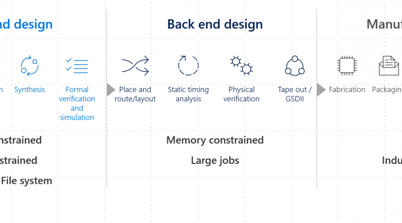
Cloud computing is enabling digital transformation across industries. Silicon, or semiconductors, are a foundational building block for the technology industry, and new opportunities are emerging in cloud computing for silicon development. The workflows for silicon development have always pushed the limits of compute, storage and networking. Over time, the silicon development flow has been greatly expanded upon to handle the increasing size, density and manufacturing complexity of the industry. This has and continues to push the envelope for high performance compute (HPC) and storage infrastructure.

Azure provides a globally available, high performance computing (HPC) platform, that is secure, reliable and scalable to meet current and emerging infrastructure needs with the silicon design and development workflow based on EDA software.
- Compute: Silicon development is compute and memory intensive. At times, it utilizes up to thousands of cores, demands the ability to quickly move and manage massive data sets for design and collaboration. Azure customers can choose from a range of compute- and memory-optimized Linux and Windows VMs to run their workflows.
- Storage: Azure Storage offers multiple storage options for handling high performance NFS scenarios in cloud-only and hybrid environments. For workflow steps like silicon RTL verification that can generate millions and millions of small (4 to 16K) temp files, Azure Avere provides high performance NFS support. Azure Avere also offers a single global namespace for hybrid or cloud-only deployment.
- Networking: Azure offers custom networking options to allow for fast, scalable, and secure network connectivity between customer premises and global Azure regions.
- Scalability: Azure offers nearly unlimited scalability. Given the cyclical nature of the silicon industry, using Azure enables organizations to rapidly increase and/or decrease the number of cores needed, while only having to pay for the resources that are used.
- Security: Azure offers a wide array of security tools and capabilities, to enable customers to secure their platform, maintain privacy and controls, meet compliance requirements, and ensure transparency.
- Global presence: Azure has more regions globally than any other cloud provider, offering the scale needed to bring applications closer to users around the world, preserving data residency, and providing comprehensive compliance and resiliency options for customers. Using Azure’s footprint, the cost, the time, and the complexity of operating a global semiconductor infrastructure can be reduced.
- Scheduling and orchestration: Azure supports commonly used tools in the silicon industry, and also provides alternatives like Azure Batch, a high-performance cloud native job scheduler. Azure CycleCloud is a site-installed, web-based orchestration tool for HPC clusters and workflows and helps create, manage, use, and optimize dynamic clustered compute environments. It can also set policies that govern access and use of Azure, which helps manage resources and costs.
Microsoft is both a developer and consumer of silicon. We are partnering with our internal silicon development organizations as well as the industry – design, manufacturing, and tools – to addressing current and emerging infrastructure needs with the silicon design and development workflow that is based on electronic design automation (EDA) software.
More detailed information on configuring Azure services for Silicon development is available in this white paper.
We look forward to sharing more details on using Azure for silicon development at DAC 2018 this week. Join us for the following sessions or contact our Silicon industry team at AzureForSilicon@microsoft.com.
- Monday, June 25, 2018 at 12:30 PM Pacific Time: “Why Cloud, Why Now”
- Monday, June 25, 2018 at 4:30 PM Pacific Time: Panel discussion – Cloud computing for EDA
- Tuesday, June 26, 2018 at 2:30 PM Pacific Time: Panel discussion – EDA on the cloud: Are we ready?
Source: Azure Blog Feed